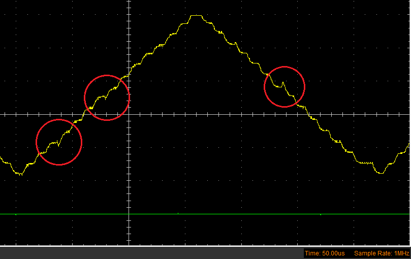
In my last post I described a cheap quaternary DAC which makes use of all four I/O pin states on the ATmega328P (including high impedance input and pull-up). The output has noticeable glitches when changing between adjacent levels, due to the weak drive from the internal and external resistors and the parasitic capacitance of the pin/protoboard.
16-level (4-bit) DAC using 2 digital I/O pins.
The resulting triangle wave shows some of the glitches for adjacent output levels.

To get a better idea of the charging delays I connected the scope directly to the output of one of the dividers and ran a set of transitions between the values.

The yellow trace shows the output level, the green pulse indicates when the pin was updated.
Some pin state transitions on the AVR require two register updates and must first go through an intermediate state (as noted in the datasheet).
The sharp edges are the transitions between driven logic levels, which are very fast. The other transitions show typical RC charging curves (exponential). Measuring the time constant I get values of roughly 2us for transitions to 'Z' (high impedance) and 1us for transitions to 'PU' (pull up activated).
For the 'Z' case, the equivalent resistance is 40kOhm, and the time constant (RC) is 2us.
This gives a parasitic capacitance of approximately 50pF.
Given these delays it is possible to stagger the updates to the pin in order to reduce the peak size of the glitch, but not to remove it entirely. It also sets the bound on the settling time of the DAC at about 5us.
The transitions to 'Z' from '0' reach 50% of the target level within about 700ns.
The transitions to 'PU' from '1' reach 50% of the target level within about 500ns.
If these delays are inserted the peak of the glitch is much smaller

The following DAC update code staggers the transitions and was used to generate the waveform, but this isn't a practical suggestion as it scratches the entire PORTD and DDRD registers.
Note: You can't use the digital pins 0&1 (the bits 0&1 of PORTD) as these have other connections on the board.
16-level (4-bit) DAC using 2 digital I/O pins.
The resulting triangle wave shows some of the glitches for adjacent output levels.
The yellow trace shows the output level, the green pulse indicates when the pin was updated.
Some pin state transitions on the AVR require two register updates and must first go through an intermediate state (as noted in the datasheet).
The sharp edges are the transitions between driven logic levels, which are very fast. The other transitions show typical RC charging curves (exponential). Measuring the time constant I get values of roughly 2us for transitions to 'Z' (high impedance) and 1us for transitions to 'PU' (pull up activated).
For the 'Z' case, the equivalent resistance is 40kOhm, and the time constant (RC) is 2us.
This gives a parasitic capacitance of approximately 50pF.
Given these delays it is possible to stagger the updates to the pin in order to reduce the peak size of the glitch, but not to remove it entirely. It also sets the bound on the settling time of the DAC at about 5us.
The transitions to 'Z' from '0' reach 50% of the target level within about 700ns.
The transitions to 'PU' from '1' reach 50% of the target level within about 500ns.
If these delays are inserted the peak of the glitch is much smaller
The following DAC update code staggers the transitions and was used to generate the waveform, but this isn't a practical suggestion as it scratches the entire PORTD and DDRD registers.
Note: You can't use the digital pins 0&1 (the bits 0&1 of PORTD) as these have other connections on the board.
| void writeDACBalanced(int n) { // implicitly using portD char dir = DACdirection[n]; char val = DACvalue[n]; // find previous code char prevDir = DDRD; char prevVal = PORTD; // is the new value a Z char toZ = (~dir)&(~val); // is the new value a PU char toPU = (~dir)&val; // intermediate timestep updates char t0Dir = prevDir & ~toZ; // clear bits which transition to Z char t0Val = prevVal & ~toZ; // clear bits which transition to Z char t1Dir = t0Dir & ~toPU; // clear bits which transition to PU char t1Val = t0Val | toPU; // set bits which transition to PU // controlled drive of output __asm__(" OUT 0x0B, %0\n\t" // t = -11 " OUT 0x0A, %1\n\t" " NOP\n\t NOP\n\t" " OUT 0x0B, %2\n\t" // t = -7 " OUT 0x0A, %3\n\t" " NOP\n\t NOP\n\t NOP\n\t NOP\n\t NOP\n\t" " OUT 0x0B, %4\n\t" // t = 0 " OUT 0x0A, %5\n\t" : : "r" (t0Val), "r" (t0Dir), "r" (t1Val), "r" (t1Dir), "r" (val), "r" (dir) : ); } |
No comments:
Post a Comment