Monday 27 April 2015

Just a bunch of resistors DAC

I needed a crude voltage reference and started connecting a few resistors to microcontroller pins. This is the simplest form of a DAC, a resistor network connected to controllable outputs. But how many levels can you create? If the pins output a binary code the upper limit would be 2^n, but microcontroller pins also have the option of a high-impedance 'input' state, increasing this to 3^n combinations.

This is a problem which has been solved many times before, there are standard solutions, such as resistor ladders (n-ary ladders, ternary and quaternary). But these often require particular resistor ratios which don't match E12 resistors, and there are problems with component tolerance. To achieve high accuracy with 1% tolerance components you need to calibrate the output and use a lookup table (not a problem with microcontroller RAM).

But what is the best result with standard 1% E12 series resistors and the smallest number of processor pins. It turns out to be a fairly computationally intensive problem because the ±1% variation in components causes ordering of output levels to swap.

The following network comes out as one of the best, achieving near 8-bits of precision using 6 microcontroller pins, 13-resistors and 1 op-amp.


The performance should be: (Based on the worst of about 100 samples in the search space of resistor tolerances)
Output: 250-levels (~8-bit)
Peak INL < 0.5 LSB
RMS INL ~ 0.15 LSB
AC Performance: Poor.

Real world results

A quick breadboard prototype with a 5.6k resistor in the output stage (to prevent saturation near the rails) gets 0.44 LSB INL for 8-bit output.


Drive and Calibration


The pins must be driven using 3-state microcontroller pins ('0','1','Z') to achieve the target number of outputs, giving 729 possible drive combinations. But not all of these patterns are actually used, only the closest to each of the 256 target levels is necessary. Due to the variation in components it isn't possible to predict which code should map to which output pattern in advance, this has to be determined for the part after assembly using an ADC. The pseudo code is roughly:


for each output pattern p (729)
   Set output pins (p)
   output_level[p] := filtered ADC

Sort(output_level)
lowest := min(output_level)
range := max(output_level)-lowest

for each target code c (256)
   ideal := lowest + (c/(256-1))*range
   lookup_table[c] := Find nearest(output_level, ideal).p

Sunday 19 April 2015

A 9-bit microcontroller DAC using a ternary resistor-ladder.


This DAC project uses the features of microcontroller I/O pins to output 512 Voltage levels (9-bit) using only 6 digital pins. It also uses calibration to achieve good linearity despite the use of 1% tolerance components in the design. (It's not going to beat a purchased DAC).

The digital I/O pins on a microcontroller generally have at least three well defined states: Output '1', Output '0' and Input (high impedance or 'Z'). (The fourth, which activates an internal pull-up-resistor, is less well defined). Using all three states the number of possible output combinations grows as 3n for n-pins, up from 2n for a binary output. For 6-pins this yields 729 possible output combinations, instead of 64 using only 2-valued logic. By using a suitable biasing circuit the three pin states can be translated to different voltage levels, which is in effect a ternary logic value. A ternary/trinary resistor-ladder makes use of these ternary values to produce a voltage output proportional to the input code (ie. a DAC).

I described some of the equations for resistor based DACs in a previous post:
Low-cost n-ary DACs using digital I/O pins.
And 'raronoff' produced a similar DAC in 2011:
The three state trinary/ ternary resistor ladder DAC.

This DAC is an example for 6-inputs with minor improvements, for the limitations skip to the end...

Improvements:
Larger biasing resistors (4.7k) reduce variation in the 'on' voltage.
A resistor ratio slightly below 4:3 ensures the output ranges for a MSB transition overlap.
Calibration and look-up table to achieve low Integral Non-Linearity (INL).

Performance:
Input pins: 6
Output resolution: 9-bits. (512-levels)
Calibrated INL < 0.5LSB (<0.44LSB measured)
Glitches ~10LSB, <100ns


Circuit Diagram


Each pin from the controller is connected to a potential divider, in this case a pair of 4.7k resistors, which hold the pin at Vs/2 when it is configured as a high impedance input. The resistors are suitably weak that the normal pin drive is unaffected, resulting in 3 possible output levels. These three-state voltage outputs are then connected to a ternary resistor-ladder DAC to produce the correctly weighted result.

Logic Pin mode V(pin)
'2' output '1' 5
'1' input (z) 2.5
'0' output '0' 0

I covered the theory for the ternary resistor-ladder in a previous post. In short the resistor ratio required is R:0.75R. This ratio is matched exactly if you have 75k and 100k resistors available. Note the resistors used on the most significant bits do not match this ideal ratio, and result in discontinuities in the output ramp. This mismatch is intentional as it allows calibration of the DAC by overlapping the ranges above and below an MSB transition, which prevents large gaps in the possible outputs.

Note: There must not be any other connections such as pull-up resistors on the board for the pins used, otherwise these will shift the 'Z' output level. On the Arduino Uno digital pins 0,1 and 13 are not suitable.

Output Buffer

It is essential to buffer the output of the DAC with a voltage follower (not shown in the diagrams). The DAC output has a variable impedance from the resistor network, and will not be linear if connected to any load! I used an MCP6292 which has a good rail-to-rail output from 2.4V to 6V.

Voltage-follower output-buffer


Breadboard prototype for the DAC.


DC Performance

On it's own this DAC will have poor performance, it's trying to achieve a 0.2% FSR output resolution with 1% tolerance resistors. The solution is to calibrate the DAC and use a lookup table to select the correct output code for each value.

To calibrate the DAC using an ADC the readings must have a low level of noise. For the example circuit I measured about 3.5mV RMS noise for both the prototype and the final board. This is very close to the size of the LSB (9-bit is approximately 10mV spacing), and so to get a stable reading an average of 256 successive samples was used. The averaged figure was stable to a higher accuracy than the 10-bit ADC.

The DAC is designed so that if the resistors have a tolerance of 1% the DAC should always be able to meet: maximum Integral Non-Linearity (INL) < 0.5 LSB at 9-bits. The INL is the measure of how much each output level differs from the ideal.

For the measured circuit he maximum difference between the ideal output value for a 9-bit DAC and the nearest existing code is approximately 4.5mV, or 0.44LSB.
Max INL = 0.44LSB   (9-bit)


INL before and after calibration.


Control Code

The DAC is more sensitive to glitches than binary designs because the transitions do not have a symmetric drive strength. It is also impossible to change both the direction and output-level of multiple pins simultaneously on some microcontrollers.

The ATMega328P used on the Arduino Uno cannot transition between input (Z) and output '1' without passing through an intermediate step, as noted in the datasheet. There are two possible intermediate states for the pin, output '0' and pull-up enabled. The pull-up state is preferred because this has a far weaker drive strength (approx 40k), and will produce a smaller glitch on the output. (It's also possible to disable pull-ups for the entire chip using the PUD control). The following update code compiles to 8 instructions not including RET.


void DACWriteTrinary(char ddrBits, char portBits)
{
     // implicit port D, no read-modify-write
     
     // optional SW glitch reduction for Z->'1'
     char zto1 = (~DDRD) & portBits;
     char viaPU = PORTD | zto1;
     
     // update registers
     __asm__("  OUT 0x0B, %2\n\t"
             "  OUT 0x0A, %0\n\t"
             "  OUT 0x0B, %1\n\t"    
     :
     : "r" (ddrBits), "r" (portBits), "r" (viaPU)
     :
   );
}


Noise Levels

The calibration routine used 180,000 samples, which gives some idea of the total system noise. Using the same board to measure the result hides variation in the USB power supply which drives both the output and the analogue reference on the ADC. (Most of the noise is probably picked up on the output line)

Noise Case RMS/mV (/LSB) Peak/mV (/LSB)
Unbuffered 2 (0.4) 12.5 (2.5)
Buffered 1.5 (0.3) 15 (3)


AC Performance

It's not stellar, but it might have some use at audio frequencies.

Ramps: 1.6µs/code to 6.8µs/code.

5kHz sine wave, approx 250kSPS.

Limitations

The 'voltage reference' for the DAC is poorly defined. It sees both the 5V supply for the driving chip, and also the internal supply voltage of the chip subject to any drop over it's input pins. Either or both of these could have significant noise, except in the case shown where the microcontroller is dedicated to driving the DAC and has no other activity.

Wednesday 15 April 2015

An 8-bit static DAC using only 4 digital I/O pins for the Arduino Uno (ATmega328P).

The Arduino Uno lacks a built in DAC, and a common project is to construct an R-2R resistor ladder DAC to output analog signals. The standard design is controlled by 8 I/O pins (8-bit) and can output up to 256 voltage levels. But using a few tricks it's possible to achieve the same number of output levels using only 4 pins.

The technique is to use all the states of a digital I/O pin, which as it's name suggests it can function both as an output and a high-impedance input. The input state also has an optional internal pull-up resistor. By selecting the right biasing circuit these extra pin states (input 'Z' and pull up 'PU') can be translated to additional output voltage levels. If these 4-state pins are connected together as part of a quaternary/4-ary resistor-ladder then the number of output levels grows as 4^n for n-inputs.

The 4-input example design can output approximately 4^4 = 256 levels (fewer after calibration). As always, it's a proof of concept. Don't use this circuit for anything serious (for a list of reasons scroll to the end).

The +12V and -12V are only necessary for the dated opamp.

The DAC Circuit


The basic unit of the circuit is a potential divider on the output of each pin which translates the four possible pin states to equally spaced voltage levels. These 4-level sources are then fed into a quaternary resistor ladder to produce the result.

One divider

The component selection must guarantee that the voltage levels at pinOutput are equally spaced. A shortcut is that if Rb1 and Rb2 are fixed as shown, Rp should be selected such that the voltage at the processor pin is 3.33V when the pull-up is enabled. (Note you can't use Arduino Uno digital pins 0,1 or 13 as these have other connections)

Output Pin States:
Logic mode DDRx PORTx v(pin) v(pinOutput)
'3' output '1' 1 1 5 2.23
'2' pull-up 0 1 3.33 1.95
'1' input (z) 0 0 1.67 1.67
'0' output '0' 1 0 0 1.39

The output from this divider is non-ideal because the equivalent source resistance varies depending on the logic level. To hide this effect the ladder should use much larger resistances, so that the variation constitutes a smaller percentage change.

The spice simulation (below) for the basic output ramp shows a number of discontinuities and glitches, even with exact component values. This is because the ratio between the two resistors in the ladder (680:330) is slightly below the ideal ratio for a quaternary DAC of 2.25:1. This mismatch is intentional, and results in a slight overlap when transitions of the most significant bits occur. These overlaps ensure that there are no large gaps in the output levels and result in better performance after calibration.


Breadboard prototype for the DAC


DC Performance

Measurements of the stable output levels using the internal ADC.


The initial run shows pretty poor linearly, but it's possible to fix most of this through calibration. The ATmega328P has sufficient RAM or flash to store a lookup table which translates between the desired output and the nearest available code.

To calibrate using the 10-bit ADC note that the readings will probably have some level of noise. I measured this to be about 3 LSB RMS for the prototype circuit. To reduce this I averaged 128 readings, resulting in a maximum variation between two successive readings of 0.7 LSB. (But it will only be as linear as the ADC.)

Its no longer possible to see the nonlinearity by eye, the Integral Non-Linearity (INL) plot is more helpful, showing an INL of ±10mV.

The DC performance can be described depending on the intended number of output levels

As an 8-bit DAC:
INL = ±0.65 LSB
DNL = -1 LSB to +0.25 LSB (duplicate codes)

As a 160-level (7.4bit) DAC:
INL = ±0.5 LSB
DNL = No duplicate codes


AC Performance

The AC performance of the DAC is fairly limited due to the parasitic capacitance of the pins and relatively large driving resistances, it's not exactly a candidate for Audio applications! The rise and fall times also vary depending on the transition, which results in visible output glitches. The following plots were produced with a samples rate of approximately 50kSPS.

Triangle waves, the left wave shows the effect of software glitch reduction from the previous post: Reducing glitches in the ladder-DAC.

Sine waves at 500Hz, 1kHz, 2kHz and 4kHz.

Square waves at 25kHz, 50kHz and 100kHz

The visible effect of the glitching can be reduced by RC-filtering the output of the DAC. The result appears much smoother when a filter with a time constant of 25uS is used. The cost of the filtering is bandwidth, square wave outputs above approximately 10kHz are significantly attenuated.


Reasons this DAC isn't practical

  1. Atmel don't want to specify the properties of the internal 'resistor' (it's not a true resistor), giving a wide range of 20k-50k. This circuit was constructed by measuring one particular chip (it's reasonably consistent between pins on the same chip, 2%).
  2. The resistor acts as if connected to a virtual source of 4.77V, not 5V. Unless the virtual source voltage scales linearly with the supply voltage any variation in the supply voltage will unset the calibration.
  3. Temperature drift is undefined.
  4. The useful bandwidth is quite limited.
The 2-pin version might have a use for a crude output level somewhere, maybe, unlikely!

Sunday 12 April 2015

Reducing the ladder-DAC glitches.

In my last post I described a cheap quaternary DAC which makes use of all four I/O pin states on the ATmega328P (including high impedance input and pull-up). The output has noticeable glitches when changing between adjacent levels, due to the weak drive from the internal and external resistors and the parasitic capacitance of the pin/protoboard.

16-level (4-bit) DAC using 2 digital I/O pins.

The resulting triangle wave shows some of the glitches for adjacent output levels.


To get a better idea of the charging delays I connected the scope directly to the output of one of the dividers and ran a set of transitions between the values.


The yellow trace shows the output level, the green pulse indicates when the pin was updated.
Some pin state transitions on the AVR require two register updates and must first go through an intermediate state (as noted in the datasheet).

The sharp edges are the transitions between driven logic levels, which are very fast. The other transitions show typical RC charging curves (exponential). Measuring the time constant I get values of roughly 2us for transitions to 'Z' (high impedance) and 1us for transitions to 'PU' (pull up activated).

For the 'Z' case, the equivalent resistance is 40kOhm, and the time constant (RC) is 2us.
This gives a parasitic capacitance of approximately 50pF.

Given these delays it is possible to stagger the updates to the pin in order to reduce the peak size of the glitch, but not to remove it entirely. It also sets the bound on the settling time of the DAC at about 5us.

The transitions to 'Z' from '0' reach 50% of the target level within about 700ns.
The transitions to 'PU' from '1' reach 50% of the target level within about 500ns.

If these delays are inserted the peak of the glitch is much smaller


The following DAC update code staggers the transitions and was used to generate the waveform, but this isn't a practical suggestion as it scratches the entire PORTD and DDRD registers.
Note: You can't use the digital pins 0&1 (the bits 0&1 of PORTD) as these have other connections on the board.

void writeDACBalanced(int n)
{
  // implicitly using portD
  char dir = DACdirection[n];
  char val = DACvalue[n];
  
  // find previous code
  char prevDir = DDRD;
  char prevVal = PORTD;

  // is the new value a Z
  char toZ = (~dir)&(~val);
  
  // is the new value a PU
  char toPU = (~dir)&val;
  
  // intermediate timestep updates
  char t0Dir = prevDir & ~toZ;  // clear bits which transition to Z
  char t0Val = prevVal & ~toZ;  // clear bits which transition to Z
  
  char t1Dir = t0Dir & ~toPU;   // clear bits which transition to PU
  char t1Val = t0Val | toPU;    // set bits which transition to PU

  // controlled drive of output
  __asm__("  OUT 0x0B, %0\n\t"                          // t = -11
          "  OUT 0x0A, %1\n\t"   
          "  NOP\n\t NOP\n\t"
          "  OUT 0x0B, %2\n\t"                          // t = -7
          "  OUT 0x0A, %3\n\t" 
          "  NOP\n\t NOP\n\t NOP\n\t NOP\n\t NOP\n\t"
          "  OUT 0x0B, %4\n\t"                          // t = 0
          "  OUT 0x0A, %5\n\t"  
     :
     : "r" (t0Val), "r" (t0Dir), "r" (t1Val), "r" (t1Dir), "r" (val), "r" (dir)
     :
   );
}

16-level (4-bit) DAC for the Arduino Uno using 2 digital I/O pins.

In my previous post I described the theory for using the additional configurations of an I/O pin (high impedance and pull-up) to produce 4 different voltage levels. This can be used to construct a 'quaternary' DAC which outputs 4^n output levels for n-inputs used, instead of the 2^n scaling for a binary ladder.

Low cost n-ary DACs using digital I/O

This circuit can output 16 different voltage levels, controlled by 2 static pins.
Note that this is not intended for any practical use! It relies on properties of the chip which are not specified to be consistent in any way, the internal pull-up 'resistors'.


If you wanted to build this you would first have to find the effective value of the internal pull-up resistors on your chip. A fast way is to find the external pull-down resistance which results in a pin voltage of exactly 3.33V when the internal pull-up is enabled. (should be somewhere 60k-100k on the ATmega328P) If this measured value is Rpulldown:
Rb2 = 0.75 Rpulldown
Rb1 = 1.5 Rpulldown


The DC performance of the DAC will vary, but it's INL is on the order of 0.25LSB.


Due to the high resistance values and slow transitions it's not as fast as an R-2R ladder, and performance falls rapidly above 10kHz. The scope capture shows a 12kHz triangle wave.


There are visible glitches when transitioning between output levels, I'll cover the solution in my next blog post.

Reducing ladder-DAC glitches.

Saturday 11 April 2015

Low-cost n-ary DACs using digital I/O pins.

There are many ways to get analogue outputs from the Arduino Uno (ATmega328P), which is otherwise limited by it's lack of an inbuilt DAC. 'Embedded newbie' did a good job of describing the different techniques in use.

Embedded newbie's blog - Review of Arduino DAC solutions (2011)

Generally the solutions can be categorised as the following:

  • Dynamic methods: Pulse Width Modulation (PWM), and capacitor integrators.
  • Static methods: Resistor ladders and networks.
  • Attaching a DAC IC via parallel or serial connection.

Most of the static designs use an R-2R resistor ladder (which is described on wiki). When a resistor ladder is used each binary code translates to a voltage level, offering 2^n output levels using n-pins of the Arduino. The exception is the cheap '2-cent' DAC which only scales linearly.

But there is always room for the esoteric and eccentric, and it's possible to build static DACs which produce more output levels per pin used. It's possible to make a 16-level (4-bit) static DAC driven from just 2-output pins (Skip to the result: 16-level DAC using 2-pins). While 16 levels might not sound like much, not all applications require high fidelity, think analogue control instead of audio reproduction!


Static DAC Designs


The '2-cent' DAC


This DAC uses a single external resistor to produce a range of output voltages. It's not very efficient as a DAC because it only scales linearly, producing (n+1) output levels for n I/O pins.

The output voltage can be calculated:


In the original description (2011) the suggested value for the external resistor was equal to the internal pull-up, but this produces a non-linear response (unless that is what you are after). Using a smaller external resistor value results in a more linear spacing of levels. This is at the lowest effort end of DACs!

2-cent DAC description


R-2R resistor ladder designs


The I/O pins from the device are connected to Vb0..3 with Vb0 representing the least significant-bit. The output is available at Vo3. The simplest way to consider the R-2R DAC is that each stage is a voltage divider of the previous stage with the ratio set to 1/2.

Considering only stage 0 (as if stages 1-3 were disconnected)


The Thevenin equivalent circuit for the first stage also has a resistance of 1R (2R||2R), so in stage 1 a further 1R is added in series to make 2R in both branches.
Ignoring the later stages (as if disconnected) and using Vo0 calculated previously


And this repeats for the final stages


This correctly weights the pins to produce an analogue approximation of a digital signal, and given that the DAC can be constructed with a single resistor value (with 2 in series or parallel to achieve the R-2R ratio) explains it's popularity.

Resistor ladder wiki.
R-2R DAC practical design.


Trinary/Ternary DACs


But it's possible to do better than this, a microprocessor pin actually has at least three states. When set as an input the pin is high impedance (effectively disconnected except for a small capacitive load). On it's own this isn't particularly useful, as the ladder-type DACs require voltage outputs, but it can be adapted using a carefully sized voltage divider. The idea was documented by 'Raronoff' in 2011.

Raronoff - Trinary/ternary ladder DAC

The adaption is biasing the pins so that when the output is in the high impedance state the voltage is held at Vs/2. The model for the pin is roughly (ignoring the drive resistance)


If the resistance Rb is large enough that it can be easily overpowered by the chip output then the equivalent model for a pin becomes as follows.

Rb must be chosen to prevent excessive current from the output when driving '1' or '0'. Raronoff suggests the absolute minimum size for Rb=120, however this causes around 40mA of current to flow through the pin, which is the absolute maximum rating. By this point the pin voltage could droop up to 1V according to the datasheet, and isn't likely to be a stable operating point. Instead a resistance of 1k and upwards will limit the output Voltage drop on the pin to a point in the linear region.

Now that the pin output looks like a three state voltage source, it can be used to construct a DAC, as described in a paper from 1979, and linked by Raronoff. This DAC can produce 3^n outputs where n is the number of input 'trits', in this case the I/O pins.

Ternary to Analog converters using resistor ladders (1979).

The biased pin is still far from an ideal voltage source, as the voltage levels have a different series resistances. The solution is to hide this as much as possible by making the resistors used in the DAC large in comparison to the bias resistors Rb.

A trinary DAC will then look something like this, I have biased the first stage to Vs/2 instead of 0.


Each stage of the DAC the should now contribute 1/3 to the next result instead of 1/2, and so the resistance ratios must be adjusted. Given a choice of Ra (which is at least an order of magnitude larger than Rb) the divider must have a ratio of 2:1.


The output can then be calculated


Here are some resistor values which provide a near linear output for a few 'trits' based on spice simulations. The 4/3 ratio isn't present in E12 resistors, but is available with E24, 75k:100k.
Ra = 75k
Rc0 = 150k
Rc = 100k
Rb = 2.2k
Rs = 25 (AVR datasheet typical)

There is an unavoidable glitch when using 'trinary' DACs on the AVR, as discovered in the original blog. For a standard R-2R DAC all of the pins can be switched with a single OUT instruction by using pins from the same PORTx register. On the AVR it is not possible to change the direction and drive-value of pins with a single instruction, resulting in a glitch output between the updates. The duration of the glitch can be minimised by ensuring that the update code uses two OUT instructions consecutively, limiting the duration to one clock period, about 63ns. Ideal solutions for removing the glitch such as a sample-and-hold circuit on the output of the DAC are overkill for a 'cheap' solution.

An example using 3-state control: A 9-bit microcontroller-driven DAC.

Quaternary/ 4-ary DAC


If I said there was more, you might guess where I was going. The Arduino I/O pins actually have 4 possible output configurations. If a '1' is written to the PORTx register when the pin is configured as an input then the internal pull-up resistor is activated. This resistor isn't exactly a precision component and will vary between chips, but it does increase the possible configurations of the pin, allowing 4^n outputs. (As I found in the previous blog post it's not even a true resistor.)

To accommodate this there is a slight change to the biasing circuit:


With the equivalent model:


In order to use this output to drive a resistor-ladder DAC the voltage levels Vs0..3 must be evenly spaced. The range of effective voltages Vs0-Vs3 might be less than the supply voltage, the full range only occurs when there is no external pin resistor (Rp=0).

By first calculating the effective voltages Vs0..3 the equations can be solved by setting Vs1 equal to 1/3 of the Vs0-Vs3 range, and Vs2 = 2/3 of the range.


The equations have a free variable, either Rp or Rb2 can be chosen. The simplest case is setting the resistor Rp=0. A non-zero Rp reduces the output range for the pin, but also has the benefit of decreasing the effective output resistance as the corresponding Rb2 will be smaller. (This ends up being significant later on, as the DAC has a high output resistance)


Which for the values measured previously (Rpu=34.4k, Vpu=4.77V) gives
Rb2 = ~60k  (59.7k)
Rb1 = ~120k (119.5k)

With these values I get the following voltages
'0' -> 0.005V - 0.010V
'1' -> 1.632V - 1.633V   (Ideal 1.667V, error=0.7% FSR)
'2' -> 3.34V - 3.35V       (Ideal 3.333V, error=0.3% FSR)
'3' -> 5.01V - 5.015V

Clearly my measurements weren't perfect, but the internal pull-up resistor isn't exactly a precision component! It's likely to vary with temperature and voltage anyway, and will be slightly different between each pin.

With Rp=0 this is far from an ideal voltage source, the series resistance varies between 25R and 40k depending on the voltage level. The ideal solution at this stage would be to buffer the resulting voltage level with an op-amp, but this doesn't really fit the Lo-Fi nature of the design. Instead the only option is to make the connected load resistor sufficiently large that the range (0-40k) appears constant, but if the resistor is too large it will have trouble driving even a small capacitive load.

The values gained by setting Rp=0 are not necessarily the most practical values. One side effect of the equations is that when driving a logic '2' using the internal pull-up resistor the voltage at the chip pin will always be 2/3 of the supply irrespective of the chosen Rp and Rb2. This simplifies characterising the value of the internal resistor to a single point on the I/V curve.

Making a DAC


Now at each stage the voltage divider should reduce the input from the previous stage to 1/4 of the full scale range. This requires an effective resistance ratio of 3:1 between the previous stage and the pin resistor.


The resistor ratio 9/4 (2.25) doesn't occur exactly, but a ratio of 2.2 is easy to achieve, and for a reason I will get to later it is better to have a ratio slightly below the target.

To construct a 2-pin DAC I used the following values:

Rc0 = 1M              (2M divider from Vs to Ground)
Ra = 330k             (8x the Rb2||Rb1 impedance)
Rc = 736k             (680k+56k, target value 742k)
Rb1 = 119k           (alternatively use 120k)
Rb2 = 60.7k          (56k + 4.7k)

The DAC is driven from digital pins 2&3 on the Arduino Uno header. It's not possible to use digital pins 0&1 because these have other connections on the board.

The output was measured by connecting it directly to an ADC input. This is not ideal because the effective output resistance of approximately 220k is too high to drive the ADC! A plot of the voltage readings used to produce the result shows a low frequency drift of about 1% FSR in addition to the noise.

The output levels look reasonably linear, as confirmed by the Integral Non-Linearity (INL):


The measured INL is about 0.22 LSB, which is 'good enough' to call this a 4-bit DAC.

AC Performance.

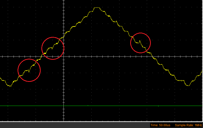
16ms ramp (31Hz triangle)
0.4ms ramp (1.2kHz triangle)
40us ramp (12kHz triangle)

The AC performance is limited to around 10kHz, possibly due to the large resistor values used in the DAC, and the effects of load and stray capacitances. For any practical purpose the DAC requires an output buffer - even connecting a cheap £5 multimeter has a significant impact on the DAC output voltage! Ideally an op-amp voltage follower on a higher supply voltage, or a voltage divider on the output.

Several glitches are visible in the transitions for the 1.2kHz triangle wave. Initially I believed these might have been due to the 63ns delay between the two instructions which update the pins (which have to be used explicitly to avoid compiler rearrangements).

__asm__( "OUT PORTD, %0 \n\t"
         "OUT DDRD, %1 \n\t"
         :
         : "r" (value), "r" (direction)
         :
       );

However increasing the delay between the two instructions doesn't lead to a corresponding increase in the glitch. The pins on the chip itself have very fast rise and fall times (on the order of 10ns), but it is possible that one of the high impedance transitions such as enabling the pull-up resistor is significantly slower in overcoming the parasitic capacitance.
Updated: the largest spikes occur with the trasnsition of the MSB from driven to high impedance, these glitches can be reduced, see:

Reducing the ladder-DAC glitches.

Extending the DAC precision.


Why stop at 2-output pins (4-bit equivalent) DAC? The answer is that these components are all poorly matched, and further bits will start to yield diminishing returns. As the number of bits increases the range will become discontinuous, with overlaps and gaps which occur when one of the MSBs transition.

There is a solution to this resolution limit, which can hide static mismatches, but not drift due to temperature. This is to design the DAC with more output levels than are required, and to calibrate and store the required codes in a lookup table. This works providing there is guaranteed to be an output voltage level within a certain range. To achieve this the potential divider equations must be revisited to guaratee that there are no gaps in the output range, which can be done by overlapping the voltage levels from the previous stage.

An example 4-state control DAC: An 8-bit static DAC using only 4 I/O pins.

It's also probably a good idea to abandon the internal pull-up resistor, the 4-ary DAC might be a novelty!